| CPC H04N 25/75 (2023.01) [H04N 25/709 (2023.01); H04N 25/772 (2023.01)] | 16 Claims |
|
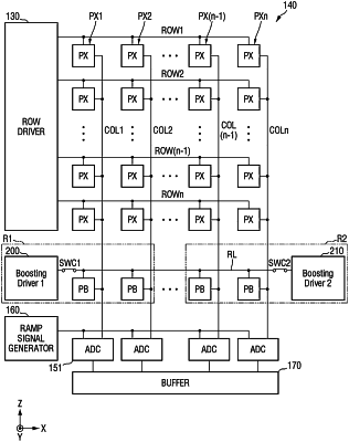
1. An image sensor, comprising:
a first row driver;
a first row line which is connected to the first row driver and extends;
a first pixel and a second pixel which are connected to the first row line;
a first column line which is connected to the first pixel and is configured to receive a first output signal from the first pixel;
a second column line which is connected to the second pixel and is configured to receive a second output signal from the second pixel;
a first boosting driver;
a second boosting driver;
a first boosting circuit connected to the first column line and configured to generate a first boosted output signal based on the first output signal and a first boosting enable signal received from the first boosting driver;
a second boosting circuit connected to the second column line and configured to generate a second boosted output signal based on the second output signal and a second boosting enable signal received from the second boosting driver;
a second row line which is connected to the first and second boosting circuits;
a first analog-digital converter (ADC) configured to receive the first boosted output signal; and
a second ADC configured to receive the second boosted output signal,
wherein the first boosting circuit is configured to adjust voltages of the first output signal,
wherein the second boosting circuit is configured to adjust voltages of the second output signal, and
wherein the first boosting driver is connected to a first terminal of the second row line and the second boosting driver is connected to a second terminal of the second row line.
|