| CPC H04N 25/46 (2023.01) [H04N 25/42 (2023.01); H04N 25/77 (2023.01)] | 20 Claims |
|
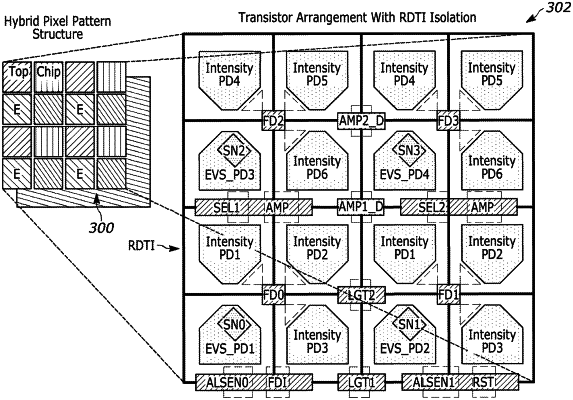
1. An imaging sensor comprising:
a pixel array including a plurality of pixel circuits; and
a plurality of binning transistors,
wherein a first portion of the plurality of pixel circuits individually includes two or more intensity photodiodes and a second portion of the plurality of pixel circuits individually includes two or more event vision sensor (EVS) photodiodes that are separate and distinct from the two or more intensity photodiodes, and
wherein the plurality of binning transistors is configured to
bin together the first portion,
bin together the second portion, and
bin together the first portion and bin together the second portion, respectively.
|