| CPC H03L 7/0807 (2013.01) [H03L 7/085 (2013.01); H04B 1/7073 (2013.01); H04L 7/0025 (2013.01); H04L 7/0331 (2013.01); H04L 27/2271 (2013.01); H04B 2201/7073 (2013.01)] | 7 Claims |

|
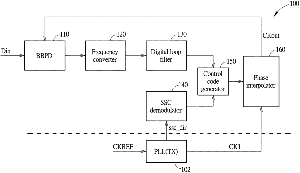
1. A circuitry, comprising:
a phase-locked loop, configured to generate a first clock signal with spread-spectrum clocking (SSC) modulation and a SSC direction signal; and
a clock and data recovery (CDR) circuit, comprising:
a phase detector, configured to compare phases of an input signal and an output clock signal to generate a detection result, wherein the input signal is with input SSC modulation;
a digital loop filter, coupled to the phase detector, configured to filter the detection result to generate a filtered signal;
a SSC demodulator, configured to receive the SSC direction signal to generate a control signal;
a control code generator, configured to generate a control code according to the filtered signal and the control signal; and
a phase interpolator, configured to use the control code to adjust a phase of the first clock signal to generate the output clock signal.
|