| CPC H03K 19/00338 (2013.01) [H03K 19/018521 (2013.01)] | 10 Claims |

|
1. A semiconductor device comprising:
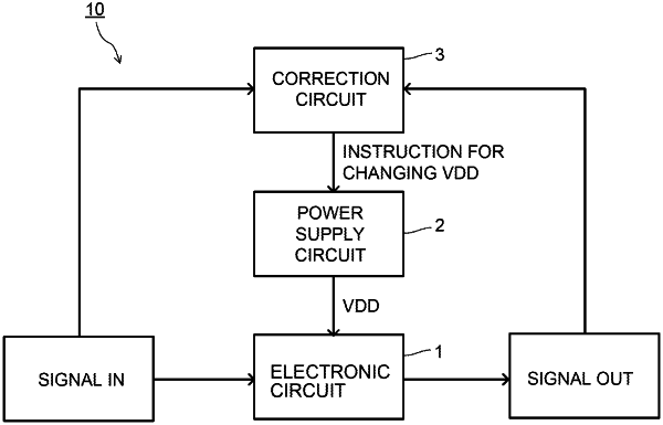
an electronic circuit configured to receive a first signal and transmit a second signal;
a power supply circuit configured to supply a power supply voltage to the electronic circuit; and
a correction circuit configured to control the power supply circuit to change a value of the power supply voltage to switch between a normal operation mode and a refresh operation mode of the device, wherein:
the electronic circuit comprises:
a first P-channel type field-effect transistor having a first gate, a first source, and a first drain, a potential of the first gate changing in response to the first signal, and a potential of one of the first source and the first drain changing in response to the power supply voltage; and
a first N-channel type field-effect transistor having a second gate, a second source, and a second drain, the second gate being electrically connected to the first gate, a potential of one of the second source and the second drain being equal to or lower than a ground potential, and another of the second source and the second drain being electrically connected to another of the first source and the first drain; and
the refresh operation mode comprises at least one operation selected from the group consisting of:
a first operation of applying a negative voltage between the first gate and at least one selected from the group consisting of the first source and the first drain so that the first gate is lower in potential than the at least one selected from the group consisting of the first source and the first drain, and applying a negative voltage between the second gate and at least one selected from the group consisting of the second source and the second drain so that the second gate is lower in potential than the at least one selected from the group consisting of the second source and the second drain;
a second operation of applying a positive voltage between the first gate and at least one selected from the group consisting of the first source and the first drain so that the first gate is higher in potential than the at least one selected from the group consisting of the first source and the first drain, and applying a positive voltage between the second gate and at least one selected from the group consisting of the second source and the second drain so that the second gate is higher in potential than the at least one selected from the group consisting of the second source and the second drain; and
a third operation of applying a voltage between the first drain and the first source, and applying a voltage between the second drain and the second source.
|