| CPC H03B 28/00 (2013.01) [G06F 1/022 (2013.01); H03H 9/19 (2013.01); H03B 2200/0034 (2013.01)] | 11 Claims |
|
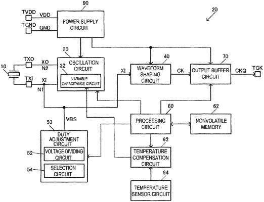
1. A circuit device comprising:
an oscillation circuit which is electrically coupled to a first node to electrically be coupled to one end of a resonator and a second node to electrically be coupled to another end of the resonator, the oscillation circuit being configured to oscillate the resonator to generate an oscillation signal, the oscillation circuit including:
an oscillation capacitor having one end coupled to the first node;
an oscillation resistor having:
one end coupled to another end of the oscillation capacitor; and
another end coupled to the second node;
a stationary capacitance capacitor having one end coupled to the first node, a capacitance value of the stationary capacitance capacitor being fixed; and
a variable capacitance element having one end coupled to another end of the stationary capacitance capacitor, a capacitance value of the variable capacitance element being variable;
a waveform shaping circuit which is coupled to the first node, to which the oscillation signal is input from the first node, and which is configured to output a clock signal obtained by performing waveform shaping on the oscillation signal; and
a duty adjustment circuit configured to:
supply the first node with a bias voltage which is variably adjusted based on adjustment data to thereby adjust a duty ratio of the clock signal; and
supply a reference voltage to the other end of the variable capacitance element.
|