| CPC H01S 5/0425 (2013.01) [H01S 5/0237 (2021.01); H01S 5/04252 (2019.08); H01S 5/18 (2013.01); H01S 5/18311 (2013.01); H01S 5/04254 (2019.08); H01S 5/423 (2013.01)] | 17 Claims |
|
1. A surface emitting laser device, comprising:
a substrate;
a first metal layer disposed on the substrate;
a second metal layer disposed on the first metal layer; and
a third metal layer disposed between the first metal layer and the second metal layer,
wherein the first to third metal layers include different materials,
wherein the second metal layer includes copper (Cu), and
wherein the third metal layer prevents diffusion of copper from the second metal layer into the first metal layer,
a first reflective layer on the third metal layer;
a light emitting layer on the first reflective layer;
an oxide layer on the light emitting layer;
a second reflective layer on the oxide layer; and
a second electrode on the second reflective layer,
wherein the second electrode includes a first metal layer, a second metal layer and a third metal layer disposed between the first metal layer and the second metal layer,
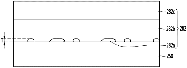
wherein the first metal layer of the second electrode includes a plurality of nanopatterns; and
wherein a separation distance between the nanopatterns is greater than or equal to a diameter of the nanopattern and is less than or equal to 3 times the diameter of the nanopatterns.
|