| CPC H01R 12/91 (2013.01) [H01R 12/716 (2013.01); H01R 13/629 (2013.01); H01R 13/6476 (2013.01); H01R 2201/18 (2013.01); H01R 2201/26 (2013.01)] | 12 Claims |

|
1. A connector comprising:
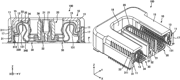
a fixed insulator;
a movable insulator that is disposed on an inner side of the fixed insulator and is movable relative to the fixed insulator; and
a plurality of contacts attached to the fixed insulator and the movable insulator, wherein
the fixed insulator comprises a plurality of first fixing grooves disposed along an arrangement direction in which the plurality of contacts are arranged, and partition walls each disposed between two corresponding adjacent ones of the contacts,
the movable insulator comprises a plurality of second fixing grooves disposed along the arrangement direction,
the contacts each comprise a first base portion supported by a corresponding one of the first fixing grooves, a second base portion supported by a corresponding one of the second fixing grooves, a first arm portion connected to the first base portion and disposed between two corresponding adjacent ones of the partition walls, and a second arm portion connected to the first arm portion and the second base portion, and
a largest width of the first arm portion is smaller than a largest width of the second arm portion.
|