| CPC H01Q 1/38 (2013.01) [H01L 21/56 (2013.01); H01L 24/26 (2013.01); H01Q 1/2283 (2013.01); H05K 2201/10098 (2013.01)] | 10 Claims |
|
1. A package, comprising:
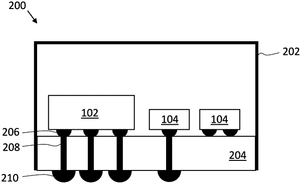
a housing, comprising a first substrate, an antenna on the first substrate, and a second substrate having a plurality of semiconductor devices thereon, wherein the first substrate is electrically connected to the second substrate by a plurality of interconnects, the plurality of interconnects vertically between the first substrate and the second substrate, and wherein the plurality of semiconductor devices and the first substrate are in a same horizontal plane;
a plurality of conductive contacts configured to electrically connect the package to other conductive contacts; and
a plurality of vias extending through the second substrate, wherein ones of the plurality of vias couple corresponding ones of the plurality of interconnect to corresponding ones of the plurality of conductive contacts.
|