| CPC H01L 33/62 (2013.01) [H01L 33/382 (2013.01); H01L 33/486 (2013.01)] | 18 Claims |

|
1. A semiconductor light-emitting element, comprising:
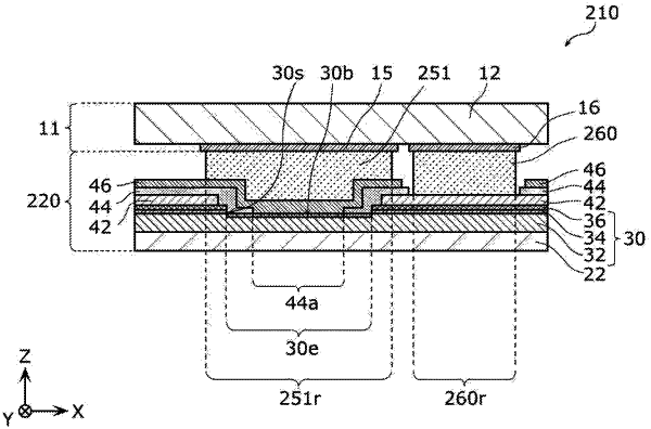
a semiconductor stack including an n-type layer, a light-emitting layer above the n-type layer, and a p-type layer above the light-emitting layer, the semiconductor stack having at least one n exposure portion which is a recess at which the n-type layer is exposed;
a p wiring electrode layer on the p-type layer;
an insulating layer that (i) continuously covers inner lateral surfaces of the at least one n exposure portion and part of a top surface of the p wiring electrode layer and (ii) has an opening portion that exposes the n-type layer at a bottom surface of the at least one n exposure portion;
an n wiring electrode layer disposed above the p-type layer and the p wiring electrode layer via the insulating layer, the n wiring electrode layer being in contact with the n-type layer in the opening portion; and
at least one first n connecting member that is a conductive member for electric connection to an external conductor, wherein:
the at least one first n connecting member is a bump made of one of Au, Ag, Al, and Cu or an alloy made of a combination of at least two of Au, Ag, Al, and Cu, and is connected to the n wiring electrode layer in at least one first n terminal region,
in a plan view, the at least one first n terminal region includes at least a portion of a region above the opening portion,
the n wiring electrode layer and the p-type layer are disposed below the at least one first n terminal region in a cross section parallel to a stacking direction of the semiconductor stack, and
a grain size of the at least one first n connecting member is larger than a grain size of the n wiring electrode layer.
|