| CPC H01L 33/58 (2013.01) [H01L 27/156 (2013.01); H01L 33/62 (2013.01)] | 9 Claims |
|
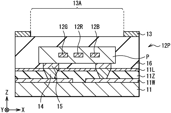
1. A display device comprising:
a substrate;
a plurality of light-emitting elements;
a first light-absorbing layer having an opening at a position that faces the plurality of light-emitting elements; and
a second light-absorbing layer that faces the first light-absorbing layer with the plurality of light-emitting elements therebetween;
a wiring line layer between the substrate and the second light-absorbing layer; and
an insulating layer between the wiring line layer and the second light-absorbing layer.
|