| CPC H01L 33/44 (2013.01) [B82B 3/0052 (2013.01); C07F 5/027 (2013.01); C07F 7/1804 (2013.01); H01L 25/0753 (2013.01); H01L 27/1214 (2013.01); H01L 33/24 (2013.01); H01L 33/38 (2013.01); H01L 33/62 (2013.01); H01L 2933/0016 (2013.01); H01L 2933/0025 (2013.01); H01L 2933/0066 (2013.01)] | 19 Claims |
|
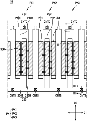
1. A light emitting element comprising:
a first conductivity type semiconductor doped to have a first polarity;
an active layer on the first conductivity type semiconductor;
a second conductivity type semiconductor on the active layer and doped to have a second polarity different from the first polarity; and
an insulating material layer surrounding side surfaces of the first conductivity type semiconductor, the second conductivity type semiconductor, and the active layer,
wherein the insulating material layer comprises an insulating material film and an element orienter bonded to an outer peripheral surface of the insulating material film.
|