| CPC H01L 33/325 (2013.01) | 13 Claims |
|
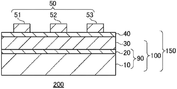
1. A group III-nitride laminated substrate comprising:
an underlying substrate;
a first layer that is formed on the underlying substrate, wherein the first layer consists of aluminum nitride, with a top surface having Al-polarity; and
a second layer that is formed on the top surface of the first layer and is made of gallium nitride,
wherein the second layer has a thickness of 10 μm or less, a half-value width of (0002) diffraction determined through X-ray rocking curve analysis is 100 seconds or less, and a half-value width of (10-12) diffraction determined through X-ray rocking curve analysis is 200 seconds or less.
|