| CPC H01L 31/12 (2013.01) [H01L 31/02005 (2013.01); H01L 31/0203 (2013.01); H01L 31/186 (2013.01)] | 20 Claims |
|
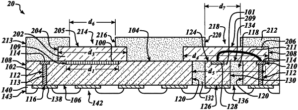
1. A device, comprising:
a sensor die having a first surface, a second surface opposite the first surface, and a sensor at the first surface;
a first opening extending into a portion of the sensor die, the first opening extending fully through the portion of the sensor die from the first surface to the second surface of the sensor die, and the first opening being spaced apart from the sensor of the sensor die;
a light emitter in the opening having a third surface substantially co-planar with the first surface of the sensor die;
an optically non-transmissive resin in the opening and on sidewalls of the light emitter, the optically non-transmissive resin extending from the first surface of the sensor die to the second surface of the sensor die, the optically non-transmissive resin including a fourth surface adjacent to the third surface; and
a first optically transmissive structure on the third surface of the light emitter and on the fourth surface of the optically non-transmissive resin.
|