| CPC H01L 29/872 (2013.01) [H01L 21/2815 (2013.01); H01L 29/0619 (2013.01); H01L 29/1608 (2013.01); H01L 29/66143 (2013.01); H01L 29/7806 (2013.01)] | 6 Claims |

|
1. A method of manufacturing a semiconductor device, comprising:
providing a substrate of a first conductivity type, the substrate having a first face and a second face;
forming a well region of a second conductivity type in the substrate such that the well region is disposed in the substrate and extends from the first face toward the second face, the second conductivity type being opposite to the first conductivity type;
forming a source region of the first conductivity type in the well region such that the source region is disposed in the well region and extends from the first face toward the second face;
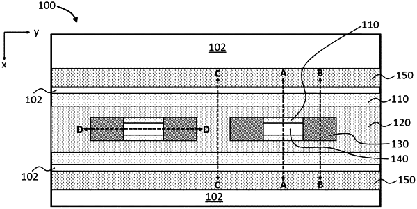
forming a Schottky region of the first conductivity type and a contact region of the second conductivity type in the substrate simultaneously such that the contact region contacts the well region and the source region, and such that in a first plane perpendicular to a direction from the first face to the second face, the Schottky region is surrounded by the well region and the contact region, wherein the boundary of the Schottky region in the first plane is in a form of quadrilateral, and a first opposite sides of the quadrilateral contact the well region, and a second opposite sides of the quadrilateral contact the contact region; and
forming a source metal layer on the first face such that a first portion of the source metal layer contacts the Schottky region to form a Schottky diode with the Schottky region, a second portion of the source metal layer forms ohmic contact with the contact region, and a third portion of the source metal layer forms ohmic contact with the source region.
|