| CPC H01L 29/861 (2013.01) [H01L 29/0634 (2013.01); H01L 29/404 (2013.01); H01L 29/0649 (2013.01)] | 20 Claims |
|
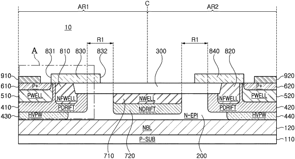
1. A semiconductor protection device comprising:
an N-type buried layer on a P-type substrate;
an N-type epitaxial layer on the N-type buried layer;
a device isolation layer on an upper surface of the N-type epitaxial layer;
an N-type drift region below the device isolation layer;
an N-type well in the N-type drift region;
first and second P-type drift regions, each of the first and second P-type drift regions in contact with a respective opposite end of the device isolation layer and spaced apart from the N-type drift region;
first and second high voltage P-type wells below the first and second P-type drift regions and in contact with the N-type buried layer;
first and second P-type wells, each of the first and second P-type wells in a respective one of the first and second P-type drift regions;
first and second N-type floating wells, each of the first and second N-type floating wells in the respective one of the first and second P-type drift regions and spaced apart from a respective one of the first and second P-type wells, and wherein each of the first and second N-type floating wells is in contact with the respective one of the opposite ends of the device isolation layer;
first and second P-type doped regions, each of the first and second P-type doped regions in the respective one of the first and second P-type wells;
a first contact layer on the N-type epitaxial layer and in contact with the first N-type floating well and the device isolation layer;
a second contact layer on the N-type epitaxial layer and in contact with the second N-type floating well and the device isolation layer;
a cathode electrode on the first P-type doped region and spaced apart from the first contact layer; and
an anode electrode on the second P-type doped region and spaced apart from the second contact layer.
|