| CPC H01L 29/7787 (2013.01) [H01L 29/15 (2013.01); H01L 29/2003 (2013.01); H01L 29/205 (2013.01); H01L 29/66462 (2013.01)] | 14 Claims |

|
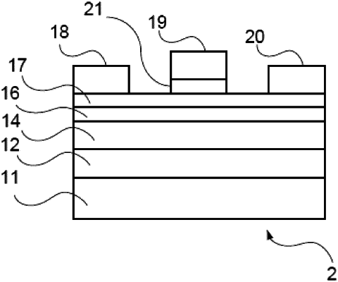
1. A heterostructure for a high electron mobility transistor (HEMT), comprising:
a SiC substrate,
an InxAlyGa1-x-yN nucleation layer, wherein x=0-1, y=0-1, formed directly on the SiC substrate, and
a GaN channel layer formed directly on the InxAlyGa1-x-yN nucleation layer, and
a barrier layer formed on the GaN channel layer,
wherein:
a thickness of the GaN channel layer is 50 to 500 nm;
a total thickness of the heterostructure, consisting of the InxAlyGa1-x-yN nucleation layer, the GaN channel layer, and the barrier layer, not including a thickness of the SiC substrate, is in a range of 54 nm to 730 nm;
the InxAlyGa1-x-yN nucleation layer is fully strained, wherein its in-plane lattice constant is exactly the same as an in-plane lattice constant of the SiC substrate, or is within +/−0.15% of an in-plane lattice constant of the SiC substrate;
the GaN channel layer presents a rocking curve with a (002) peak having a full width half maximum (FWHM) below 300 arcsec, and a rocking curve with a (102) peak having a FWHM below 400 arcsec as determined by X-ray diffraction (XRD); and
a surface of the GaN channel layer of the heterostructure prior to formation of any additional layers thereon exhibits root mean square (RMS) roughness of below 1.8 nm over a 10×10 μm2 scan area, or of below 1 nm over a 3×3 μm2 scan area.
|