| CPC H01L 29/7786 (2013.01) [H01L 21/02389 (2013.01); H01L 21/02433 (2013.01); H01L 29/04 (2013.01); H01L 29/2003 (2013.01); H01L 29/66431 (2013.01)] | 17 Claims |
|
1. A method for manufacturing a nitride-based high electron mobility transistor, comprising:
providing a conductive member on a nitride semiconductor crystal substrate, outside an element region of the high electron mobility transistor in a plan view;
forming a mask on the nitride semiconductor crystal substrate, the mask having an opening in at least one of a source recess etching region where a source recess is formed, which is a recess in which a source electrode of the high electron mobility transistor is arranged, and a drain recess etching region where a drain recess is formed, which is a recess in which a drain electrode of the high electron mobility transistor is arranged;
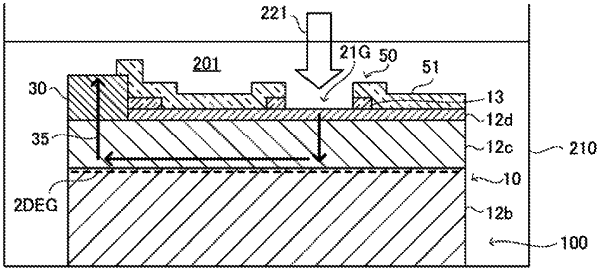
performing photoelectrochemical etching by irradiating the nitride semiconductor crystal substrate with light to form at least one of a source recess and a drain recess, in a state where the nitride semiconductor crystal substrate on which the conductive member is provided and the mask is formed is in contact with an etching solution containing an oxidizing agent that receives electrons; and
forming an element separation structure of the high electron mobility transistor,
wherein the nitride semiconductor crystal substrate includes on a base substrate, at least: a channel layer on which a two-dimensional electron gas is formed, a barrier layer formed on the channel layer, and a cap layer formed on the barrier layer, which is composed of a group III nitride having a bandgap smaller than that of a group III nitride constituting the barrier layer,
in the photoelectrochemical etching, the cap layer is removed, and
the conductive member is electrically connected to the source recess etching region or the drain recess etching region through at least one of the cap layer and the two-dimensional electron gas.
|