| CPC H01L 29/7786 (2013.01) [H01L 29/66462 (2013.01); H01L 29/7787 (2013.01)] | 24 Claims |
|
1. A high electron mobility transistor comprising:
a channel layer comprising a 2-dimensional electron gas (2DEG);
a barrier layer on the channel layer and comprising first regions and a second region, the first regions on portions of the channel layer and configured to induce the 2DEG of a first density in the portions of the channel layer, and the second region on other portions of the channel layer and configured to induce the 2DEG of a second density different from the first density in the other portions of the channel layer;
source and drain electrodes on the barrier layer; and
a gate electrode on the barrier layer between the source and drain electrodes,
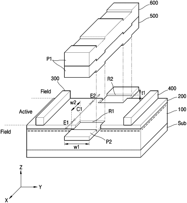
the first regions including a first edge region and a second edge region opposite each other with the second region in between,
the first edge region and the second edge region corresponding respectively to both a first end and a second end of a surface of the channel layer crossing the gate electrode in plan view, wherein
the barrier layer includes recesses in the first edge region and the second edge region,
a thickness of the barrier layer in the recesses is greater than 0 nm and less than a thickness of the barrier layer in the second region,
a portion of the gate electrode vertically overlapping the recesses is closer to the surface of the channel layer than a part of the gate electrode over the second region of the barrier layer,
the second region is not recessed,
the source electrode and the drain electrode each have a longest dimension that extends parallel to each other in a first direction,
the gate electrode has a longest dimension that extends in the first direction parallel to the longest dimension of each of the source electrode and drain electrode, and
the first edge region and the second edge region are separated from each other in the first direction by the second region.
|