| CPC H01L 29/66969 (2013.01) [H01L 27/1225 (2013.01); H01L 29/045 (2013.01); H01L 29/24 (2013.01); H01L 29/41733 (2013.01); H01L 29/4908 (2013.01); H01L 29/78618 (2013.01); H01L 29/78648 (2013.01); H01L 29/7869 (2013.01); H01L 29/78696 (2013.01); H01L 29/7849 (2013.01); H01L 29/786 (2013.01)] | 13 Claims |
|
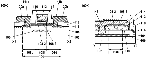
1. A semiconductor device comprising:
a conductive film;
a first insulating film over the conductive film;
an oxide semiconductor film over the first insulating film;
a second insulating film over the oxide semiconductor film;
a metal oxide film over the second insulating film;
a gate electrode over the metal oxide film; and
a third insulating film over the gate electrode,
wherein the oxide semiconductor film comprises a channel region overlapping with the gate electrode, a source region in contact with the third insulating film, and a drain region in contact with the third insulating film,
wherein the second insulating film comprises a nitride,
wherein the metal oxide film comprises at least one of In, Zn, Al, Ga, Y, and Sn,
wherein the third insulating film is in contact with a top surface and a side surface of the gate electrode, a side surface of the metal oxide film, a side surface of the second insulating film, and a part of a top surface of the oxide semiconductor film, and
wherein the gate electrode is in contact with the conductive film through an opening in the first insulating film, the second insulating film and the metal oxide film.
|