| CPC H01L 29/4975 (2013.01) [H01L 21/28 (2013.01); H01L 21/823431 (2013.01); H01L 21/823475 (2013.01); H01L 27/0886 (2013.01); H01L 27/092 (2013.01); H01L 29/41775 (2013.01); H01L 29/66477 (2013.01); H01L 29/783 (2013.01)] | 16 Claims |
|
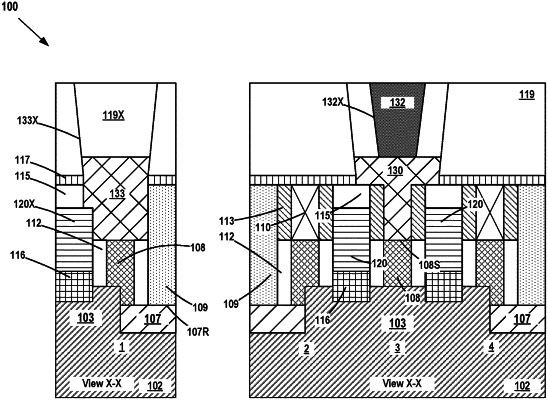
1. An integrated circuit (IC) product, comprising:
a first conductive source/drain contact structure of a first transistor;
an insulating source/drain cap positioned above at least a portion of an upper surface of the first conductive source/drain contact structure, wherein the insulating source/drain cap physically contacts the upper surface of the first conductive source/drain contact structure;
a gate-to-source/drain (GSD) contact structure that is conductively coupled to the first conductive source/drain contact structure and a first gate structure of a second transistor, wherein an upper surface of the GSD contact structure is positioned at a first level that is at a level that is below a level of an upper surface of the insulating source/drain cap, and wherein the GSD contact structure physically contacts a side surface of the insulating source/drain cap, a side surface of the first conductive source/drain contact structure, and a top surface of the first conductive source/drain contact structure; and
a gate contact structure that is conductively coupled to a second gate structure of a third transistor, the third transistor including a second conductive source/drain contact structure and a second insulating source/drain cap positioned above an upper surface of the second conductive source/drain contact structure, wherein the gate contact structure physically contacts an upper surface of the second insulating source/drain cap of the third transistor, wherein an upper surface of the gate contact structure is positioned at a second level that is at a level that is above the first level.
|