| CPC H01L 29/458 (2013.01) [H01L 27/124 (2013.01); H01L 29/401 (2013.01); H01L 29/4908 (2013.01); H10K 10/82 (2023.02); H10K 10/84 (2023.02); H10K 71/236 (2023.02); H10K 71/621 (2023.02); Y10S 438/937 (2013.01)] | 9 Claims |
|
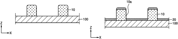
1. A method of manufacturing a display device, the method comprising:
forming a photoresist layer on a substrate by applying and patterning a photosensitive material on the substrate, the photoresist layer exposing first portions of the substrate;
forming a first conductive layer on the photoresist layer and the first portions of the substrate, the first conductive layer comprising a first metal material;
etching a side surface of the photoresist layer having the first conductive layer thereon to expose second portions of the substrate;
forming a second conductive layer on the first conductive layer on the photoresist layer of which the side surface is etched, on the first conductive layer on the first portions of the substrate, and on the second portions of the substrate, the second conductive layer comprising a second metal material having a Young's modulus greater than that of the first metal material; and
removing the photoresist layer to form the second conductive layer covering the first conductive layer on the first portions of the substrate, the first conductive layer covered by the second conductive layer forming a conductive wiring of the display device.
|