| CPC H01L 29/41733 (2013.01) [H01L 27/0688 (2013.01); H01L 27/092 (2013.01); H01L 29/0665 (2013.01); H01L 29/41783 (2013.01); H01L 29/42392 (2013.01); H01L 29/78621 (2013.01); H10B 10/125 (2023.02); H10B 10/18 (2023.02)] | 16 Claims |
|
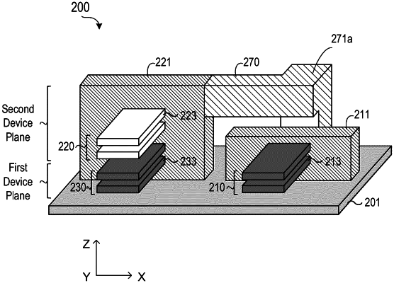
1. A semiconductor device, comprising:
a first device plane over a substrate, the first device plane including a first transistor device having a first source/drain (S/D) region formed in an S/D channel;
a second device plane over the first device plane, the second device plane including a second transistor device having a second gate formed in a gate channel which is adjacent to the S/D channel; and
a first inter-level connection from the first S/D region of the first transistor device to the second gate of the second transistor device, wherein the first inter-level connection includes a lateral offset from the S/D channel to the gate channel, wherein
the first inter-level connection comprises the S/D channel, a horizontal portion that contacts the S/D channel, and a vertical portion that connects the horizontal portion to the second gate, and
the vertical portion extends from the first device plane to the second device plane and corresponds to a vertical distance from the first S/D region to the second gate relative to a surface of the substrate.
|