| CPC H01L 29/267 (2013.01) [H01L 29/40111 (2019.08); H01L 29/516 (2013.01); H01L 29/6684 (2013.01); H01L 29/78391 (2014.09)] | 12 Claims |

|
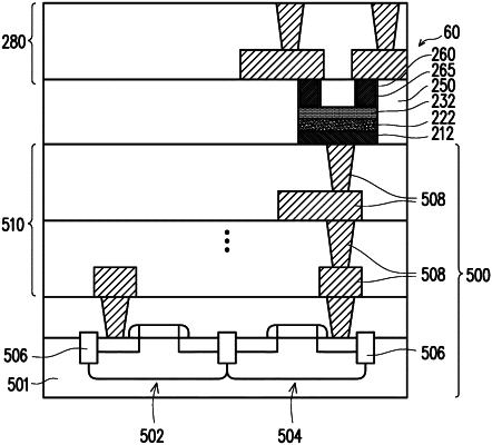
1. A semiconductor device, comprising:
a gate layer;
a semiconductor layer;
a ferroelectric layer disposed between the gate layer and the semiconductor layer,
wherein the semiconductor layer includes a first material containing a Group III element, a rare-earth element and a Group VI element, the ferroelectric layer includes a second material containing a Group III element, a rare-earth element and a Group V element and the gate layer includes a third material containing a Group III element and a rare-earth element; and
source and drain terminals being in direct contact with the semiconductor layer, wherein a topmost position of an interface between the semiconductor layer and the ferroelectric layer is lower than top surfaces of the source and drain terminals, and
wherein a content of the rare-earth element in the semiconductor layer gradually varies from a first side of the semiconductor layer to a second side of the semiconductor layer.
|