| CPC H01L 29/2003 (2013.01) [H01L 29/0607 (2013.01); H01L 29/404 (2013.01); H01L 29/407 (2013.01); H01L 29/4236 (2013.01); H01L 29/7786 (2013.01)] | 20 Claims |
|
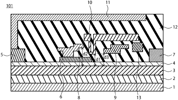
1. A semiconductor device, comprising:
a first nitride semiconductor layer;
a second nitride semiconductor layer on a surface of the first nitride semiconductor layer and having a larger bandgap than the first nitride semiconductor layer;
a first electrode on the second nitride semiconductor layer and electrically connected to the first nitride semiconductor layer;
a second electrode on the first nitride semiconductor layer and electrically connected to the first nitride semiconductor layer;
a gate electrode including a planar portion between the first electrode and the second electrode in a first direction parallel to the surface of the first nitride semiconductor layer;
a gate field plate electrode on the gate electrode and electrically connected to the gate electrode, the gate field plate electrode including a central portion directly above the gate electrode in a second direction that is orthogonal to the surface of the first nitride layer;
a first field plate electrode above the second nitride semiconductor layer in the second direction at a position that is between the gate field plate electrode and the second electrode in the first direction, the first field plate electrode being electrically connected to the first electrode; and
a second field plate electrode including an upper planar portion and a projecting portion that extends from the upper planar portion towards the first nitride semiconductor layer in the second direction, the projecting portion being between the first field plate electrode and the gate field plate electrode in the first direction, and electrically connected to the first electrode, wherein
a distance from the first nitride semiconductor layer to a bottom surface of the projecting portion of the second field plate electrode is shorter than a distance from the first nitride semiconductor layer to a bottom surface of an outermost end portion of the gate field plate electrode that protrudes the most in the first direction towards a second electrode side,
the distance from the first nitride semiconductor layer to the bottom surface of the projecting portion of the second field plate electrode is greater than zero but shorter than a distance from the first nitride semiconductor layer to a bottom portion of an end surface of the first field plate electrode on a first electrode side,
the bottom surface of the projecting portion of the second field plate electrode is separated from the second nitride semiconductor layer by an interlayer insulation layer, and
an end portion of the planar portion of the gate electrode is overlapped with the projecting portion of the second field plate electrode in the second direction and between the projecting portion of the second field plate electrode and the second nitride semiconductor layer in the second direction.
|