| CPC H01L 29/1037 (2013.01) [H01L 21/3081 (2013.01); H01L 21/3086 (2013.01); H01L 29/7827 (2013.01)] | 25 Claims |
|
1. A method of forming a semiconductor structure, comprising:
forming a first array of mandrels on a hardmask layer disposed on an uppermost surface of a semiconductor substrate;
forming first sidewall image transfer spacers on opposing longitudinal sidewalls of each mandrel in the first array of mandrels;
forming a second array of mandrels on the hardmask layer, each mandrel in the second array of mandrels being laterally separated from each mandrel in the first array of mandrels by the first sidewall image transfer spacers;
forming second sidewall image transfer spacers on opposing transversal sidewalls of the first array of mandrels and the second array of mandrels; and
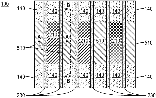
selectively removing portions of the second sidewall image transfer spacers to define a crosslink fin pattern.
|
|
6. A method of forming a semiconductor structure, comprising:
patterning a plurality of fin structures on an uppermost surface of a semiconductor substrate, each fin structure of the plurality of fin structures including n first regions extending perpendicular to the uppermost surface of the semiconductor substrate and n-1 second regions extending between and connecting each of the n first regions and parallel to the uppermost surface of the semiconductor substrate, wherein n≤1.
|
|
12. A method of forming a semiconductor structure comprising:
forming a hardmask layer on an uppermost surface of a semiconductor substrate; and
transferring a pattern to the hardmask layer to define a plurality of fin structures on the uppermost surface of the semiconductor substrate, the plurality of fins structures including one or more vertical regions extending in a direction perpendicular to the uppermost surface of the semiconductor substrate and parallel to one another, at least two vertical regions of the one or more vertical regions being connected by a horizontal region extending between the at least two vertical regions in a direction parallel to the uppermost surface of the semiconductor substrate.
|