| CPC H01L 27/156 (2013.01) [H01L 33/005 (2013.01); H01L 33/24 (2013.01); H01L 33/38 (2013.01); H01L 33/44 (2013.01)] | 20 Claims |
|
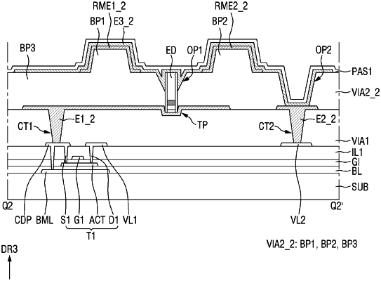
1. A display device comprising:
a first via layer disposed on a substrate and comprising trench parts recessed from an upper surface of the first via layer;
a first electrode and a second electrode that are disposed on the first via layer and spaced apart from each other;
a second via layer disposed on the first via layer and comprising:
first openings partially exposing the first electrode; and
a second opening partially exposing the second electrode;
light emitting elements disposed in the first openings of the second via layer and extending in a direction; and
a third electrode disposed on the second via layer, wherein
each of the light emitting elements includes:
a first end electrically connected to the first electrode; and
a second end electrically connected to the third electrode, and
each of the light emitting elements is disposed such that the extending direction of the light emitting elements is not parallel to an upper surface of the substrate.
|