US 12,002,836 B2
Pixel with strained silicon layer for improving carrier mobility and blue response in imagers
Chandra Mouli, Boise, ID (US)
Assigned to Micron Technology, Inc., Boise, ID (US)
Filed by Micron Technology, Inc., Boise, ID (US)
Filed on Jan. 21, 2021, as Appl. No. 17/154,703.
Application 12/942,044 is a division of application No. 12/344,740, filed on Dec. 29, 2008, granted, now 7,872,284, issued on Jan. 18, 2011.
Application 17/154,703 is a continuation of application No. 16/161,653, filed on Oct. 16, 2018, granted, now 10,910,431.
Application 16/161,653 is a continuation of application No. 15/284,232, filed on Oct. 3, 2016, granted, now 10,134,798, issued on Nov. 20, 2018.
Application 15/284,232 is a continuation of application No. 12/942,044, filed on Nov. 9, 2010, granted, now 9,461,079, issued on Oct. 4, 2016.
Application 12/344,740 is a continuation of application No. 11/590,761, filed on Nov. 1, 2006, granted, now 7,485,904, issued on Feb. 3, 2009.
Application 11/590,761 is a continuation of application No. 10/612,974, filed on Jul. 7, 2003, granted, now 7,164,182, issued on Jan. 16, 2007.
Prior Publication US 2021/0242272 A1, Aug. 5, 2021
Int. Cl. H01L 27/146 (2006.01); H01L 31/0352 (2006.01); H01L 31/11 (2006.01)
CPC H01L 27/14647 (2013.01) [H01L 27/14603 (2013.01); H01L 27/14609 (2013.01); H01L 27/1461 (2013.01); H01L 27/14689 (2013.01); H01L 31/0352 (2013.01); H01L 27/14652 (2013.01); H01L 31/11 (2013.01)] 20 Claims
OG exemplary drawing
 
1. A system, comprising:
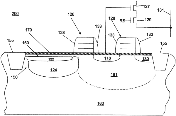
an imaging device including at least one pixel cell having a photosensor with a photosensitive region buried at least in part within a substrate such that the photosensitive region is separated from a strained silicon layer by an intermediary portion of the substrate;
a central processing unit operably connected to the imaging device via a first bus; and
a memory component operably connected to the central processing unit via a second bus, wherein:
the memory component is configured to (i) receive, via the first bus or the second bus, a digital image from the imaging device and (ii) store the digital image, and
the central processing unit is configured to (a) receive, via the second bus, the digital image from the memory component and (b) process the digital image.