| CPC H01L 27/14636 (2013.01) [H01L 27/14603 (2013.01); H01L 27/14609 (2013.01); H01L 27/1464 (2013.01)] | 13 Claims |
|
1. A light detecting device, comprising:
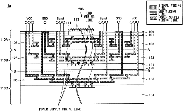
a first substrate including a first semiconductor substrate and a first wiring layer, the first semiconductor substrate having a pixel;
a second substrate including a second semiconductor substrate and a second wiring layer, the second semiconductor substrate having a first circuit;
a third substrate including a third semiconductor substrate and a third wiring layer, the third semiconductor substrate having a second circuit;
a first coupling structure, wherein the first coupling structure includes a via that extends through the second semiconductor substrate, wherein the first coupling structure electrically connects a first wiring of the first wiring layer to a first wiring of the second wiring layer; and
an electrode junction structure, wherein the electrode junction structure connects the second wiring layer to the third wiring layer, wherein the electrode junction structure includes a second wiring of the second wiring layer and a first wiring of the third wiring layer, wherein a portion of the second wiring of the second wiring layer is exposed at a surface of the second wiring layer, wherein a portion of the first wiring of the third wiring layer is exposed at a surface of the third wiring layer, and wherein at least a portion of the exposed portion of the second wiring of the second wiring layer is in contact with at least a portion of the exposed portion of the third wiring layer.
|