| CPC H01L 27/14636 (2013.01) [H01L 27/14683 (2013.01)] | 20 Claims |
|
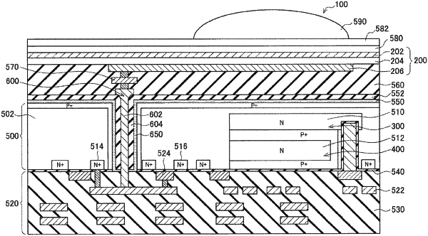
1. A solid-state image sensor, comprising:
a semiconductor substrate;
a charge accumulator disposed in the semiconductor substrate and configured to accumulate charge;
a photoelectric converter disposed above the semiconductor substrate and configured to convert light to charge; and
a through electrode passing through the semiconductor substrate and electrically connecting the charge accumulator with the photoelectric converter,
wherein, at an end portion on a photoelectric converter side of the through electrode, a cross-sectional area of a conductor positioned at a center of the through electrode in a cut section orthogonal to a through direction of the through electrode gradually increases toward the photoelectric converter along the through direction, and
wherein, in a cross section of the through electrode cut along the through direction, an end portion on a photoelectric converter side of the conductor has two first branch portions split from a center axis of the conductor.
|