| CPC H01L 27/14634 (2013.01) [H01L 24/05 (2013.01); H01L 24/08 (2013.01); H01L 27/14636 (2013.01); H01L 2224/05553 (2013.01); H01L 2224/08146 (2013.01)] | 14 Claims |
|
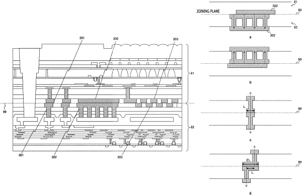
1. A semiconductor device, comprising:
a first semiconductor substrate including a first multilayer wiring layer; and
a second semiconductor substrate including a second multilayer wiring layer, wherein the first semiconductor substrate and the second semiconductor substrate are joined together with the first multilayer wiring layer and the second multilayer wiring layer directly connected to each other to form a plurality of conductors in a proximity of a joining plane of the of the first and second semiconductor substrates, wherein connection holes are formed in either or both of the first multilayer wiring layer and the second multilayer wiring layer, wherein rivets are fitted to the connection holes, and wherein the plurality of conductors are electrified in a direction of the joining plane.
|