| CPC H01L 27/14618 (2013.01) [H01L 27/14621 (2013.01); H01L 27/14627 (2013.01); H01L 27/14636 (2013.01); H01L 27/14645 (2013.01); H01L 27/14683 (2013.01)] | 20 Claims |
|
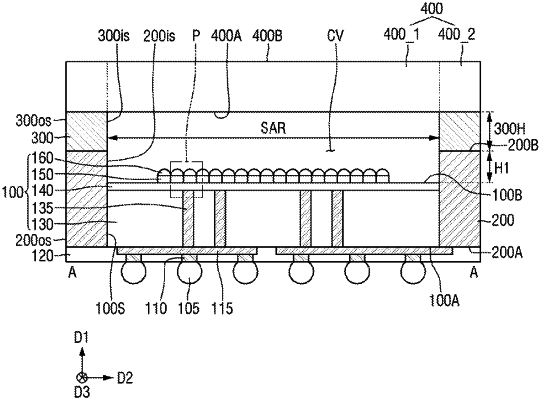
1. An image sensor package comprising:
an image sensor chip including:
first and second faces that are opposite to each other; and
side walls connecting the first and second faces;
a mold layer disposed on the side walls of the image sensor chip and including third and fourth faces that are opposite to each other;
a transparent substrate disposed on the second face of the image sensor chip and spaced apart from the image sensor chip in a first direction, the transparent substrate including a first portion that overlaps the image sensor chip in the first direction and a second portion that does not overlap the image sensor chip in the first direction; and
an adhesive layer disposed between the mold layer and the second portion of the transparent substrate,
wherein the side walls of the image sensor chip overlap the mold layer in a second direction intersecting the first direction, and
the fourth face of the mold layer does not overlap the image sensor chip in the first direction.
|