| CPC H01L 27/14614 (2013.01) [H01L 27/14616 (2013.01); H01L 27/14638 (2013.01); H01L 27/14643 (2013.01); H01L 27/14647 (2013.01); H01L 27/14667 (2013.01); H04N 25/60 (2023.01); H04N 25/76 (2023.01); H10K 19/00 (2023.02); H10K 39/32 (2023.02)] | 16 Claims |
|
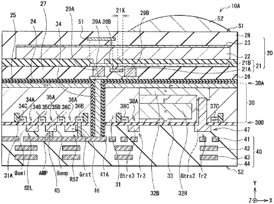
1. A solid-state imaging element, comprising:
a first electrode including a plurality of electrodes, wherein the plurality of electrodes includes a charge accumulation electrode and a charge readout electrode;
a second electrode opposed to the first electrode; and
a photoelectric conversion layer between the first electrode and the second electrode, wherein
the first electrode has, at least in a portion, a first overlap section where the charge accumulation electrode overlaps with the charge readout electrode with a first insulation layer interposed therebetween,
the charge accumulation electrode is configured to accumulate a charge generated in the photoelectric conversion layer, and
the charge readout electrode is configured to readout the charge generated in the photoelectric conversion layer.
|