| CPC H01L 27/1461 (2013.01) [H01L 27/14621 (2013.01); H01L 27/14623 (2013.01); H01L 27/14627 (2013.01); H01L 27/1463 (2013.01); H01L 27/14645 (2013.01)] | 11 Claims |
|
1. A solid-state imaging device comprising:
a semiconductor substrate having one surface and another surface opposed to the one surface;
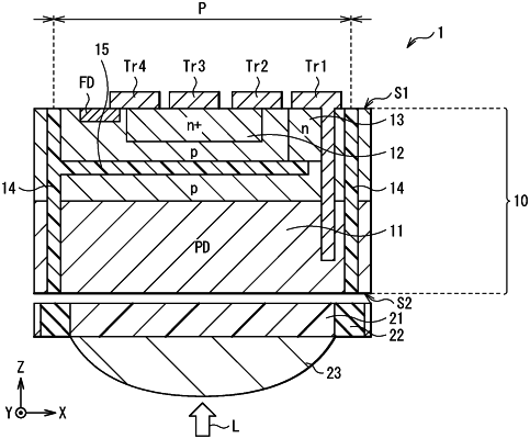
a photoelectric conversion section formed to be embedded in the semiconductor substrate;
a charge holding section provided in the one surface of the semiconductor substrate while being stacked on the photoelectric conversion section;
an n-type semiconductor region provided in the one surface of the semiconductor substrate; and
a charge-voltage conversion section provided in the one surface of the semiconductor substrate,
wherein a charge generated in the photoelectric conversion section is transferred via the n-type semiconductor region to the charge holding section,
wherein the n-type semiconductor region extends to a position between the photoelectric conversion section and the charge holding section, and
wherein the charge holding section is surrounded by the n-type semiconductor region.
|