| CPC H01L 27/14609 (2013.01) [H01L 27/14645 (2013.01); H04N 25/778 (2023.01); H10K 39/32 (2023.02)] | 19 Claims |
|
1. A solid-state image sensor comprising:
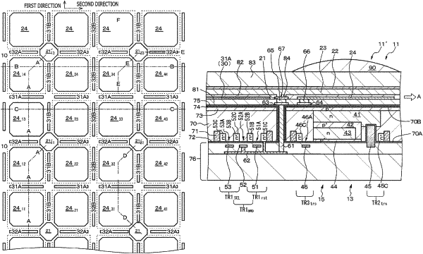
a plurality of imaging device blocks each including P×Q (where P≥2, Q≥1) imaging devices, wherein
each of the imaging devices includes a photoelectric conversion portion that includes a photoelectric conversion layer, an insulating layer, and a charge accumulating electrode arranged opposed to the photoelectric conversion layer with an insulating layer interposed therebetween,
in each of the imaging device blocks, a first charge movement controlling electrode is provided between the imaging devices,
a second charge movement controlling electrode is provided between the imaging device blocks,
in the imaging device blocks, P imaging devices are arrayed along a first direction, and Q imaging device is arrayed along a second direction, and
charge accumulated in the photoelectric conversion layer of a (P−1)th imaging device from a first imaging device along the first direction is transferred to the photoelectric conversion layer of a Pth imaging device and read out together with charge accumulated in the photoelectric conversion layers of Q Pth imaging devices, under control of the first charge movement controlling electrode.
|