| CPC H01L 27/1288 (2013.01) [H01L 25/167 (2013.01); H01L 27/124 (2013.01); H01L 27/1248 (2013.01); H10K 59/124 (2023.02); H10K 59/131 (2023.02); H10K 71/00 (2023.02); H10K 59/1201 (2023.02)] | 25 Claims |
|
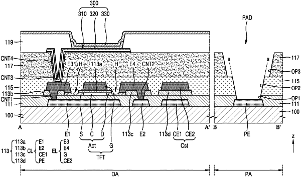
1. A display apparatus comprising:
a substrate comprising a display area and a peripheral area adjacent to the display area;
a thin-film transistor located in the display area of the substrate, and comprising:
a semiconductor layer; and
a gate electrode overlapping a channel region of the semiconductor layer;
a conductive layer disposed between the substrate and the semiconductor layer, and comprising:
a first electrode located in the display area of the substrate; and
a pad electrode located in the peripheral area of the substrate,
a first insulating layer disposed between the conductive layer and the semiconductor layer and having a first opening that exposes at least a portion of an upper surface of the pad electrode;
a second insulating layer disposed on the gate electrode of the thin-film transistor and having a second opening coinciding with the first opening of the first insulating layer, the gate electrode being disposed between the second insulating layer and the substrate; and
a pixel electrode disposed over the second insulting layer and electrically connected to the thin-film transistor.
|