| CPC H01L 27/1251 (2013.01) [H01L 27/124 (2013.01); H01L 29/78633 (2013.01); H01L 27/1225 (2013.01)] | 16 Claims |
|
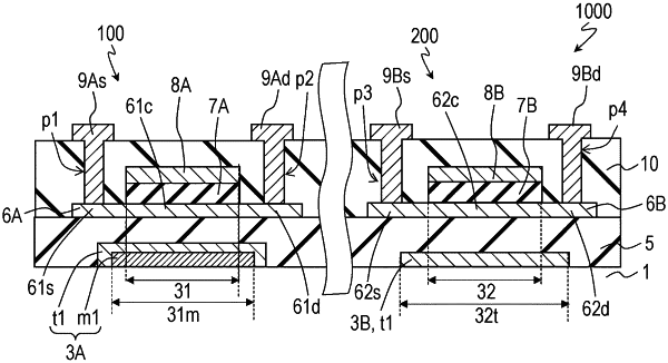
1. An active matrix substrate comprising:
a substrate; and
a plurality of oxide semiconductor TFTs supported on the substrate, wherein:
the plurality of oxide semiconductor TFTs include a plurality of first TFTs and a plurality of second TFTs,
each of the first TFTs includes a first lower electrode, a first insulating layer that covers the first lower electrode, a first oxide semiconductor layer disposed on the first insulating layer, and a first gate electrode disposed on a portion of the first oxide semiconductor layer with a first gate insulating layer therebetween,
in each of the first TFTs,
the first oxide semiconductor layer includes a first channel region that overlaps the first gate electrode when viewed in a normal direction of the substrate, and
the first lower electrode has a first light-shielding portion that overlaps an entirety of the first channel region when viewed in the normal direction of the substrate, and the first light-shielding portion includes a first metal film,
each of the second TFTs includes a second lower electrode, the first insulating layer that is extended to cover the second lower electrode, a second oxide semiconductor layer disposed on the first insulating layer, and a second gate electrode disposed on a portion of the second oxide semiconductor layer with a second gate insulating layer therebetween, and
in each of the second TFTs,
the second oxide semiconductor layer includes a second channel region that overlaps the second gate electrode when viewed in the normal direction of the substrate, and
the second lower electrode has a light-transmitting portion that overlaps at least a portion of the second channel region when viewed in the normal direction of the substrate, and the light-transmitting portion includes a first transparent conductive film but not a light-shielding metal film.
|