| CPC H01L 27/124 (2013.01) [H01L 27/1259 (2013.01)] | 20 Claims |
|
1. A display substrate, comprising:
a base substrate having a first display region and a second display region, wherein the first display region is at least partially disposed around the second display region; and
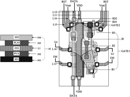
a plurality of pixels, each comprising a pixel circuit and a target electrode connected to each other, wherein the pixel circuit is disposed in one of the first display region and the second display region, and the target electrode is disposed in the second display region; and the pixel circuit comprises a first metal layer, a first insulating layer, at least one transparent conductive line, a second insulating layer, and a second metal layer which are disposed on a side of the base substrate and sequentially stacked, each of the at least one transparent conductive line being connected to one metal layer in the pixel circuit.
|