| CPC H01L 27/124 (2013.01) [H01L 25/162 (2013.01); H01L 25/167 (2013.01); H01L 27/1262 (2013.01); H10K 59/131 (2023.02); H10K 59/18 (2023.02)] | 24 Claims |
|
1. A display device comprising:
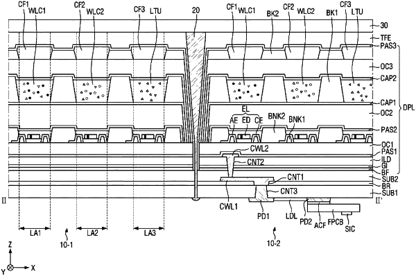
a first substrate, wherein a first contact hole is defined in the first substrate;
a barrier layer disposed on the first substrate, wherein a second contact hole is defined in the barrier layer and is connected to the first contact hole;
a first connection line disposed on the barrier layer and inserted into the second contact hole;
a second substrate covering the first connection line and the barrier layer;
a thin-film transistor layer disposed on the second substrate and including at least one thin-film transistor; and
a pad part disposed on a lower surface of the first substrate and connected to the first connection line through the first contact hole,
wherein the thin-film transistor layer further has a second connection line connected between the first connection line and the at least one thin-film transistor, and the first connection line extends in a layer between the barrier layer and the second substrate.
|