| CPC H01L 27/124 (2013.01) [H01L 24/05 (2013.01); H01L 27/1218 (2013.01); H01L 27/1266 (2013.01); H01L 24/08 (2013.01); H01L 24/32 (2013.01); H01L 24/80 (2013.01); H01L 24/83 (2013.01); H01L 25/167 (2013.01); H01L 27/156 (2013.01); H01L 2224/05541 (2013.01); H01L 2224/05571 (2013.01); H01L 2224/08225 (2013.01); H01L 2224/32225 (2013.01); H01L 2224/80203 (2013.01); H01L 2224/80801 (2013.01); H01L 2224/83203 (2013.01); H01L 2224/83851 (2013.01); H10K 59/131 (2023.02)] | 11 Claims |
|
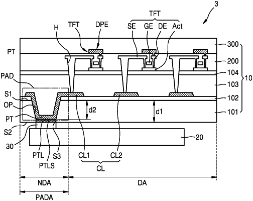
1. A display device comprising a display area and a non-display area, the display device further comprising:
a base layer comprising a first surface and a second surface opposite to the first surface, the base layer having, in the non-display area, an opening portion penetrating the first surface and the second surface;
a pad unit comprising a terminal on the first surface of the base layer, the terminal extending from the first surface of the base layer to the opening portion, and forming at least one side of the opening portion;
a connection line connected to the terminal on the first surface, the connection line extending from the non-display area to the display area;
an insulating layer covering the terminal and the connection line;
a thin-film transistor comprising a semiconductor layer on the insulating layer, the thin-film transistor being connected to the connection line; and
a display element connected to the thin-film transistor, the display element being in the display area,
wherein the first surface of the base layer faces the display element, and
wherein the insulating layer is located between the connection line and the semiconductor layer, and fills the opening portion.
|