| CPC H01L 27/0727 (2013.01) [H01L 29/0619 (2013.01); H01L 29/0692 (2013.01); H01L 29/0696 (2013.01); H01L 29/66136 (2013.01); H01L 29/66348 (2013.01); H01L 29/7397 (2013.01); H01L 29/861 (2013.01); H01L 29/8613 (2013.01)] | 13 Claims |
|
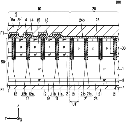
1. A reverse conducting semiconductor device having an insulated gate bipolar transistor region and a diode region, the reverse conducting semiconductor device comprising:
a semiconductor substrate included in the insulated gate bipolar transistor region and the diode region, the semiconductor substrate having a first principal surface and a second principal surface opposite to the first principal surface, the semiconductor substrate including
a drift layer extending over the insulated gate bipolar transistor region and the diode region and having a first conductivity type,
a base layer arranged between the drift layer and the first principal surface in the insulated gate bipolar transistor region, the base layer having a second conductivity type different from the first conductivity type,
an emitter layer arranged between the base layer and the first principal surface in the insulated gate bipolar transistor region, the emitter layer having the first conductivity type,
a base contact layer arranged between the base layer and the first principal surface in the insulated gate bipolar transistor region, the base contact layer forming a part of the first principal surface, the base contact layer having the second conductivity type,
a collector layer arranged between the drift layer and the second principal surface in the insulated gate bipolar transistor region, the collector layer having the second conductivity type,
an anode layer arranged between the drift layer and the first principal surface in the diode region, the anode layer having the second conductivity type,
an anode contact region arranged between the anode layer and the first principal surface in the diode region, the anode contact region forming a part of the first principal surface, the anode contact region having a second conductivity type impurity concentration peak value higher than that of the anode layer, the anode contact region having the second conductivity type, and
a cathode layer arranged between the drift layer and the second principal surface in the diode region, the cathode layer having the first conductivity type;
an insulated gate structure for forming, with the base layer, a channel for controlling an electrical path between the emitter layer and the drift layer;
a collector electrode electrically connected to the collector layer and the cathode layer; and
an emitter electrode in contact with the base contact layer and the anode contact region,
wherein the anode contact region includes a first anode contact layer having a lower net concentration and a higher first conductivity type impurity concentration than the base contact layer.
|
|
11. A method for manufacturing a reverse conducting semiconductor device for manufacturing the reverse conducting semiconductor device according to claim 1, the method comprising:
performing first conductivity type impurity doping of the emitter layer by ion implantation into the first principal surface of the semiconductor substrate; and
performing first conductivity type impurity doping of the first anode contact layer by ion implantation into the first principal surface of the semiconductor substrate,
wherein the first conductivity type impurity doping of the emitter layer and the first conductivity type impurity doping of the first anode contact layer are simultaneously performed as a common first conductivity type impurity doping.
|