| CPC H01L 25/18 (2013.01) [H01L 25/0657 (2013.01); H01L 2225/06524 (2013.01); H01L 2225/06548 (2013.01)] | 9 Claims |

|
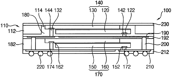
1. A method of manufacturing a fan-out type semiconductor package, the method comprising:
arranging an upper chip stack in a cavity of a frame;
forming a first redistribution pattern under the frame, the first redistribution pattern electrically connected with the upper chip stack;
arranging a lower chip stack under the first redistribution pattern;
forming a second redistribution pattern under the lower chip stack, the second redistribution pattern electrically connected with the lower chip stack; and
electrically connecting the first redistribution pattern and the second redistribution pattern with each other using a redistribution post,
wherein arranging the upper chip stack in the cavity comprises stacking a second upper chip, which has a size substantially the same as a size of a first upper chip, on an upper surface of the first upper chip in a step-like shape to expose a first upper pad on an edge portion of the first upper chip, which is not overlapped with the second upper chip, and to expose a second upper pad on an edge portion of the second upper chip, which is not overlapped with the first upper chip.
|