| CPC H01L 25/167 (2013.01) [H01L 27/156 (2013.01); H01L 33/56 (2013.01); H01L 33/62 (2013.01)] | 19 Claims |

|
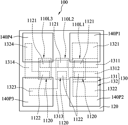
1. An LED device comprising:
a plurality of LED chips, each of said LED chips having opposite first and second surfaces, and a side surface that is connected between said first and second surfaces, and including a semiconductor stack having a first-type semiconductor layer, a second-type semiconductor layer, and a light-emitting layer located between the first semiconductor layer and the second semiconductor layer, and an electrode assembly disposed on the semiconductor stack and including a first electrode and a second electrode, wherein the first electrode is electrically connected to the first semiconductor layer, and the second electrode is electrically connected to the second semiconductor layer;
an electric circuit layer assembly disposed on said second surfaces of said LED chips, and having opposite first and second surfaces and a side surface that is connected between said first and second surfaces of said electric circuit layer assembly, said first surface of said electric circuit layer assembly being directly and electrically connected to said first and second electrodes of said electrode assembly;
an encapsulating layer enclosing said LED chips and said electric circuit layer assembly in such a manner that at least a portion of said second surface of said electric circuit layer assembly is exposed from said encapsulating layer; and
a plurality of bond pads that are disposed on said encapsulating layer and that are electrically connected to said electric circuit layer assembly,
wherein a total surface area of said bond pads is greater than a total surface area of said first surfaces of said LED chips.
|