| CPC H01L 25/167 (2013.01) [H01L 33/483 (2013.01); H01L 33/60 (2013.01); H01L 33/62 (2013.01)] | 15 Claims |
|
1. A light-emitting diode device, comprising:
a substrate having opposite upper and lower surfaces, and four edges that are interconnected to one another and that surround said upper surface;
an electrically conductive layer formed on said upper surface of said substrate, and having a first region and a second region that are electrically separated from each other by a trench structure, said trench structure having a first segment that is inclined relative to each of said edges of said substrate by a predetermined angle larger than 0 degrees and smaller than 90 degrees, and a second segment that is connected to said first segment;
a first light-emitting diode chip disposed across said first segment of said trench structure and interconnecting said first and second regions of said electrically conductive layer; and
an anti-electrostatic discharge element disposed across said second segment of said trench structure and interconnecting said first and second regions of said electrically conductive layer;
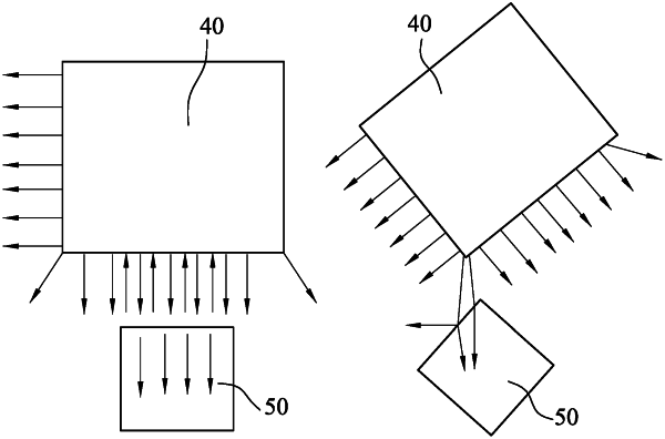
wherein each of said first light-emitting diode chip and said anti-electrostatic discharge element has side surfaces and edges interconnecting said side surfaces, one of said side surfaces of said first light-emitting diode chip nearest said anti-electrostatic discharge element having normal lines that intersect with all points on a nearest one of said side surfaces of said anti-electrostatic discharge element, an intersecting angle between any one of said normal lines and said nearest one of said side surfaces of said anti-electrostatic discharge element being not equal to 90°;
wherein said first light-emitting diode chip does not have a side surface having normal lines that intersect with all points on the nearest one of said side surfaces of said anti-electrostatic discharge element, and an intersecting angle between each of said normal lines and said nearest one of said side surfaces of said anti-electrostatic discharge element is equal to 90°;
wherein each of a projection of said first light-emitting diode chip on said electrically conductive layer and a projection of said anti-electrostatic discharge element on said electrically conductive layer has a substantially rectangular shape;
wherein the projection of said anti-electrostatic discharge element has a first vertex at a distance from a nearest one of vertices of the projection of said first light-emitting diode chip nearest said anti-electrostatic discharge element that is smaller than a distance from each of the remaining vertices of the projection of said anti-electrostatic discharge element to said nearest one of said vertices of the projection of said first light-emitting diode chip;
wherein said distance between said first vertex of the projection of said anti-electrostatic discharge element and said nearest one of said vertices of the projection of said first light-emitting diode chip is not smaller than 0.2 mm; and
wherein the projection of said anti-electrostatic discharge element has a second vertex and a third vertex neighboring said first vertex of the projection of said anti-electrostatic discharge element, and an included angle defined between a first imaginary line that connects said second vertex and a centroid of said first light-emitting diode chip and a second imaginary line that connects said third vertex and said centroid of said first light-emitting diode chip is not smaller than 5° and not greater than 36°.
|