| CPC H01L 25/0753 (2013.01) [H01L 21/68 (2013.01); H01L 33/0093 (2020.05)] | 18 Claims |
|
1. A system for transferring alignment marks between substrate systems comprising:
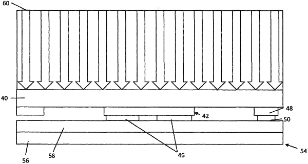
a substrate comprising a plurality of semiconductor devices and a plurality of alignment marks in alignment with the semiconductor devices, the alignment marks comprising physical structures that can be physically transferred between substrate systems; and
a first substrate system comprising a temporary substrate having an adhesive layer thereon configured to contact and apply adhesive forces to the semiconductor devices and the alignment marks, the temporary substrate configured to support and bond with the semiconductor devices and the alignment marks while maintaining the alignment between the semiconductor devices and the alignment marks, the adhesive layer configured to maintain the adhesive forces during bonding and separating of the substrate from the temporary substrate.
|