| CPC H01L 25/0753 (2013.01) [H01L 33/62 (2013.01); H01L 2933/0066 (2013.01)] | 20 Claims |
|
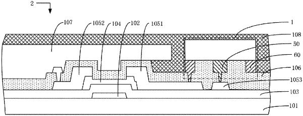
1. A light emitting device, comprising:
a first substrate;
a N-type contact layer disposed on the first substrate;
an active layer disposed on the N-type contact layer; and
a P-type contact layer disposed on the active layer;
wherein a first electrode and a second electrode arranged around the first electrode are disposed on the P-type contact layer, in response to the first electrode being an N-type electrode and the second electrode being a P-type electrode, the first electrode is connected to the N-type contact layer through a via hole, or in response to the first electrode being a P-type electrode and the second electrode being an N-type electrode, the second electrode is connected to the N-type contact layer through a via hole; and
wherein a first encapsulation layer is disposed at a side of the second electrode away from the first electrode, and the first encapsulation layer is arranged around the second electrode.
|