| CPC H01L 25/0753 (2013.01) [H01L 27/1214 (2013.01); H01L 33/38 (2013.01); H01L 33/44 (2013.01); H01L 33/62 (2013.01)] | 22 Claims |
|
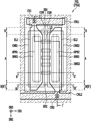
1. A pixel comprising:
a first electrode and a second electrode facing each other;
an insulating layer on the first and second electrodes;
a plurality of light-emitting elements located on the insulating layer between the first electrode and the second electrode;
a first contact electrode electrically connected to the first electrode; and
a second contact electrode electrically connected to the second electrode,
wherein a first gap having a constant width in a first direction and a second gap having a width in the first direction that gradually changes along a second direction are located between the first electrode and the second electrode or between the first contact electrode and the second contact electrode, the second direction being crossing the first direction.
|