| CPC H01L 25/0657 (2013.01) [H01L 23/3128 (2013.01); H01L 23/3171 (2013.01); H01L 24/06 (2013.01); H01L 24/16 (2013.01); H01L 24/17 (2013.01); H01L 24/81 (2013.01); H01L 25/50 (2013.01); H01L 2224/06515 (2013.01); H01L 2224/16145 (2013.01); H01L 2224/16225 (2013.01); H01L 2224/1703 (2013.01); H01L 2224/81815 (2013.01)] | 9 Claims |
|
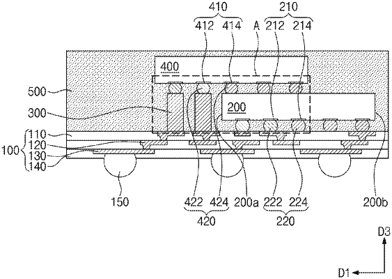
1. A semiconductor package, comprising:
a first semiconductor chip mounted on a substrate in a flip-chip bonding manner;
a first conductive post disposed on the substrate and spaced apart from the first semiconductor chip, the first conductive post extending vertically to couple to the substrate;
a second semiconductor chip disposed on the first semiconductor chip and the first conductive post, the second semiconductor chip including a signal pad and a dummy pad on a bottom surface of the second semiconductor chip; and
a mold layer on the substrate that covers the first semiconductor chip, the second semiconductor chip, and the first conductive post,
wherein the second semiconductor chip is supported on the first semiconductor chip by a first dummy solder terminal, and the first dummy solder terminal is between the first semiconductor chip and the dummy pad of the second semiconductor chip,
the second semiconductor chip is coupled to the first conductive post by a first signal solder terminal, and the first signal solder terminal is between the first conductive post and the dummy pad of the second semiconductor chip,
the first dummy solder terminal is in direct contact with a top surface of the first semiconductor chip, and is electrically disconnected from the second semiconductor chip,
the signal pad, the first signal solder terminal and the first conductive post are vertically aligned,
the first dummy solder terminal and the first signal solder terminal include solder balls or solder bumps,
the top surface of the first semiconductor chip and a top surface of the first conductive post are located at different levels from a top surface of the substrate, and
a height difference between the top surface of the first semiconductor chip and the top surface of the first conductive post measured from the substrate is smaller than a first height of the first signal solder terminal and a second height of the first dummy solder terminal.
|