| CPC H01L 25/0652 (2013.01) [H01L 23/3128 (2013.01); H01L 23/3135 (2013.01); H01L 23/367 (2013.01); H01L 23/481 (2013.01); H01L 23/5383 (2013.01); H01L 23/5385 (2013.01)] | 18 Claims |
|
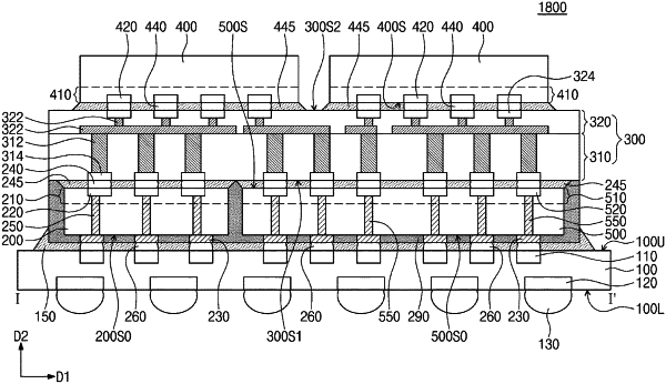
1. A semiconductor package comprising:
an upper substrate having a first surface and a second surface opposite to each other,
a lower semiconductor chip on the first surface of the upper substrate;
a plurality of conductive pillars on the first surface of the upper substrate and at least one side of the lower semiconductor chip;
a lower mold layer on the first surface of the upper substrate, the lower mold layer filling a space between the lower semiconductor chip and the plurality of conductive pillars;
a plurality of upper semiconductor chips on the second surface of the upper substrate, the plurality of upper semiconductor chips include a first upper semiconductor chip and a second upper semiconductor chip laterally spaced apart from each other in a first direction parallel to the second surface of the upper substrate and electrically connected to the second surface of the upper substrate;
upper bumps between the first upper semiconductor chip and the second surface of the upper substrate and the second upper semiconductor chip and the second surface of the upper substrate; and
upper underfill layers respectively disposed between the first upper semiconductor chip and the second surface of the upper substrate and the second upper semiconductor chip and the second surface of the upper substrate,
wherein the lower semiconductor chip vertically overlaps a portion of the first upper semiconductor chip and a portion of the second upper semiconductor chip in a second direction perpendicular to the second surface of the upper substrate,
wherein the lower semiconductor chip includes lower through-electrodes penetrating therethrough, one of the lower through-electrodes vertically overlaps the portion of the first upper semiconductor chip in the second direction, and another of the lower through-electrodes vertically overlaps the portion of the second upper semiconductor chip in the second direction,
wherein the upper underfill layers are laterally spaced apart from each other in the first direction, and each of the upper underfill layers covers corresponding ones of the upper bumps,
wherein the lower semiconductor chip and the plurality of conductive pillars are electrically connected to the first surface of the upper substrate.
|