| CPC H01L 24/81 (2013.01) [H01L 24/05 (2013.01); H01L 24/11 (2013.01); H01L 24/13 (2013.01); H01L 2224/0401 (2013.01); H01L 2224/05555 (2013.01); H01L 2224/10175 (2013.01); H01L 2224/11013 (2013.01); H01L 2224/1146 (2013.01); H01L 2224/13018 (2013.01); H01L 2224/13019 (2013.01); H01L 2224/13076 (2013.01); H01L 2224/13147 (2013.01); H01L 2224/16135 (2013.01); H01L 2224/16268 (2013.01); H01L 2224/81385 (2013.01); H01L 2224/81815 (2013.01); H01L 2924/01047 (2013.01); H01L 2924/0105 (2013.01); H01L 2924/01079 (2013.01); H01L 2924/014 (2013.01)] | 20 Claims |
|
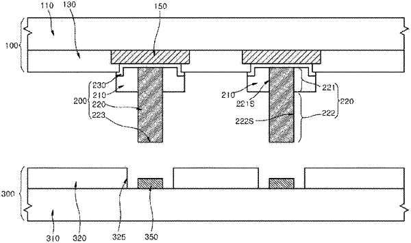
1. A method of manufacturing a semiconductor device, the method comprising:
forming a substrate including a connection pad;
forming a first resist pattern on the connection pad of the substrate, the first resist pattern including a ring-shaped first opening;
forming a ring pattern of a solder layer with an inserting hole by filling the ring-shaped first opening with a solder material;
selectively removing a portion of the first resist pattern that fills the inserting hole;
forming a second resist pattern with a second opening that substantially overlaps with the inserting hole; and
filling the second opening with a metal material to form a metal post, the metal post with an inserting portion that is inserted into the inserting hole and a protruding portion that protrudes outside of the ring pattern of the solder layer.
|