| CPC H01L 24/03 (2013.01) [H01L 21/02164 (2013.01); H01L 21/0217 (2013.01); H01L 21/02271 (2013.01); H01L 21/02274 (2013.01); H01L 21/76837 (2013.01); H01L 23/3171 (2013.01); H01L 23/3192 (2013.01); H01L 24/11 (2013.01); H01L 2224/0391 (2013.01); H01L 2224/1191 (2013.01); H01L 2924/30205 (2013.01)] | 20 Claims |
|
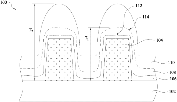
1. A method of making a semiconductor device, the method comprising:
depositing a dielectric layer over a conductive pad using a first deposition process; and
depositing a first passivation layer directly over the dielectric layer using a high density plasma chemical vapor deposition (HDPCVD), wherein the first deposition process is different from HDPCVD.
|